Description
Epitaxy of wafers: The basis of numerous components
You can rely on our experience and strict quality control in the epitaxial growth of MOCVD layer structures.
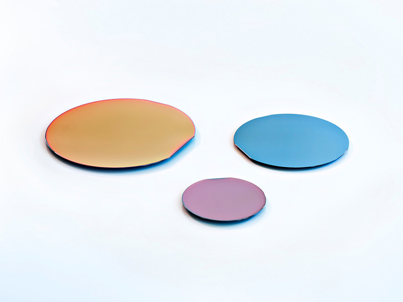
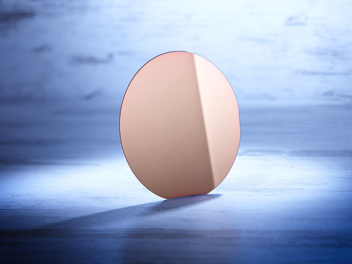
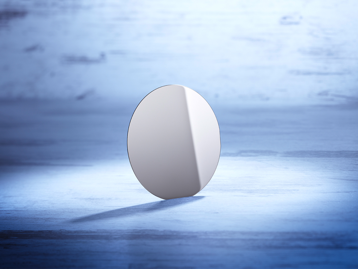
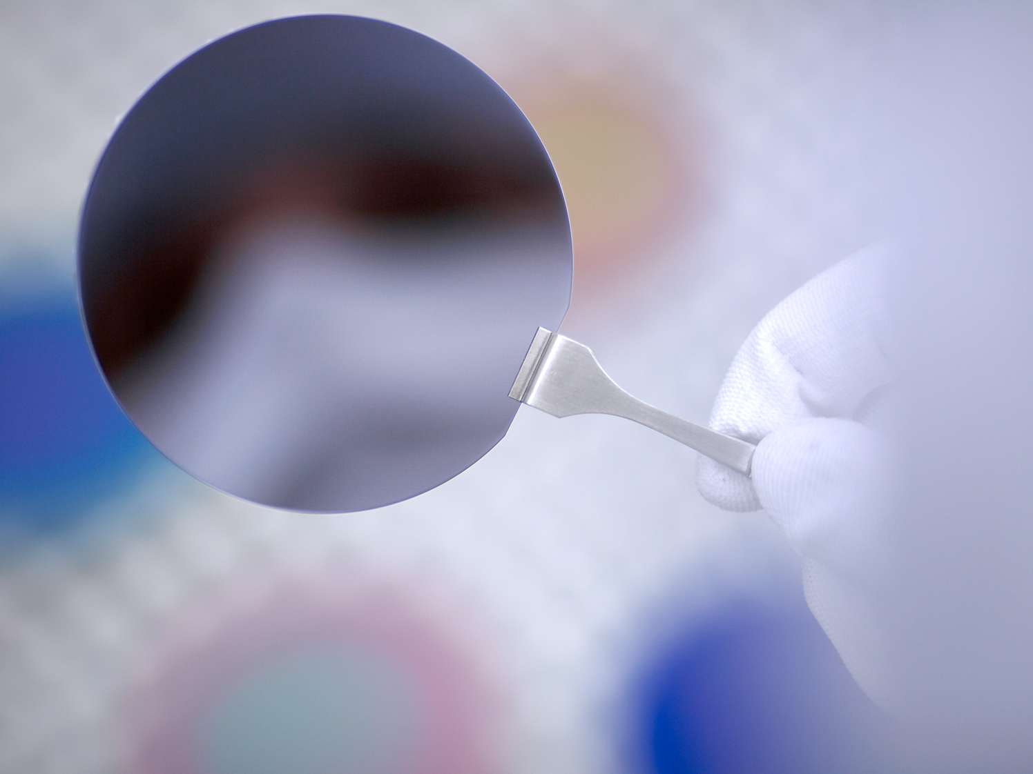
The production of various components is based on the epitaxy of wafers. Depending on your design, Jenoptik produce semiconductor layer structures on 2-inch, 3-inch, 4 -inch and 6-inch wafers. Two different reactors with 8 or 12 wafers per run are used to produce the wafers.
The wafers coated in this way by means of epitaxial growth can be used for semiconductor components in numerous units and systems: In high-power diode lasers within a wavelength range of currently 760 to 1060 nanometers as surface emitters (VCSELs and VECSELs), as light-emitting diodes (RCLEDs and LEDs) or as detectors.
The MOCVD/MOVPE growth process is extremely reliable and is monitored closely. In this way, a high quality in the epitaxy of wafers is consistently ensured. This process is certified according to the international standard ISO 9001:2008.
Jenoptik’s engineers and technicians have continuously enhanced the process over many years. The epitaxy of wafers is therefore one of Jenoptik’s specialist competencies.


